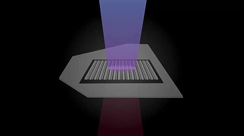
Researchers at Columbia University have made significant strides in the field of quantum technologies by shrinking nonlinear optical platforms to a mere 160 nanometers. This breakthrough, detailed in a paper published in Nature Photonics in October 2025, involves the use of metasurfaces—artificial structures etched into ultrathin crystals—which enhance optical properties at the nanoscale.
The team, led by Jim Schuck, a professor of mechanical engineering, initially developed a method for creating entangled photon pairs using a crystalline device just 3.4 micrometers thick. This foundational work is essential for advancing quantum technologies, which rely on the generation of qubits—quantum bits that form the building blocks of quantum computing.
Innovative Techniques in Nonlinear Optics
In their recent research, the Columbia engineers focused on transition metal dichalcogenides (TMDs), a class of crystals that can be peeled into atom-thin layers. These materials exhibit significant nonlinearity, but until now, were too thin to efficiently produce photons with new frequencies. According to Chiara Trovatello, an assistant professor at Politecnico di Milano and a former Marie Skłodowska-Curie Global Fellow at Columbia, “For quantum technologies, like quantum processors, size becomes crucial.”
The researchers employed a technique known as periodic poling to optimize the optical output by layering the TMD molybdenum disulfide in alternating directions. This arrangement allowed light waves traveling through each layer to be phase-matched, preventing interference. In their latest findings, the team introduced highly tunable, etched metasurfaces to enhance the nonlinear optical effects further.
Nanoscale Enhancements and Practical Applications
The new metasurfaces allow researchers to alter the optical properties of the crystals in unprecedented ways. By etching a series of repeating lines onto the surface of molybdenum disulfide, Zhi Hao Peng, a Ph.D. student and the first author of the study, reported enhancements in the process known as second-harmonic generation. This effect, where two photons merge into one with double the frequency and half the wavelength, was boosted nearly 150 times compared to unpatterned samples.
The implications of this work extend beyond theoretical advancements. As quantum technologies continue to evolve, the need for smaller, more efficient qubit sources becomes imperative. Current quantum devices require substantial space, often occupying entire rooms. Trovatello emphasized, “To make quantum technologies scalable, we need to shrink the size of our qubit sources.”
The research not only establishes a new methodology for enhancing optical properties but also paves the way for integrating these innovations into existing telecommunications networks. The light produced operates at telecommunications-range wavelengths, making it compatible with current devices.
“This could be one of the most compact sources of entangled photons at that wavelength range,” remarked Schuck, highlighting the potential for fully on-chip quantum photonics.
As the research progresses, the team is now focused on reversing the second-harmonic generation process—splitting one photon into two entangled photons. The simplicity of Peng’s etching technique makes it easier and more cost-effective than previous methods, which often involved complex and brittle materials.
The collaborative efforts of theoretical physicists, such as Andrea Alu and his former postdoctoral researcher Michele Cortufo, have also contributed to determining the optimal metasurface pattern necessary to achieve these remarkable efficiencies.
In summary, the advancements made by the Columbia team represent a pivotal step toward realizing compact, efficient quantum technologies. As they continue to refine their techniques, the potential for practical applications in quantum computing and telecommunications looks increasingly promising.


